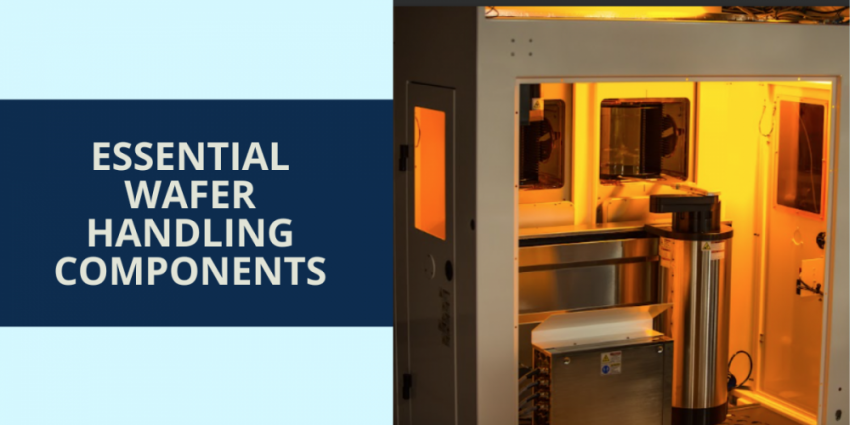
There is no space for mistake in semiconductor fabrication. A single scratch, a speck of dust, or a little vibration might ruin a wafer that costs thousands of dollars. When yield rates decide how much money a business makes, the machines that move these fragile substrates become the most important part of the fabrication operation. Areliable wafer handling system does more than merely transport silicon from one place to another; it also keeps the product safe at every stage.
The most important things to fab managers and process engineers are cleanliness and stability. Knowing what goes into these automated solutions makes it easier to choose the correct tools for production. Every little thing, from robotic kinematics to the end-effectors’ material science, affects the ultimate throughput. Here is a list of the parts that make up a system that works well.
Precision Robotics and Kinematics
The core of any wafer transfer system is the robotic arm. This mechanism is responsible for transporting wafers between cassettes, process modules, and alignment stations. Reliability here means smooth motion profiles. Jerky movements or sudden stops create vibrations that can dislodge a wafer or generate microscopic particles through friction.
High-quality semiconductor automation equipment utilizes direct-drive technology. Unlike belt-driven systems, direct-drive motors reduce backlash and wear over time. This leads to higher repeatability, meaning the robot returns to the exact same position within microns, cycle after cycle. Consistent positioning prevents collisions and scratching, keeping the wafer handling automation process safe.
Advanced End-Effector Technology
The end-effector, or the “hand” of the robot, makes direct contact with the substrate. This component presents the highest risk for contamination or physical damage. Engineers must choose between vacuum grip, edge grip, or Bernoulli handling depending on the application. Vacuum grippers are standard for the backside of wafers, but can leave marks. Edge grippers hold the wafer along its perimeter, protecting the active area but requiring precise calibration.
For thinned or warped wafers, wafer handling technology often employs Bernoulli grippers. These use airflow to create a pressure differential, allowing the wafer to float without contact. Selecting the correct gripping method minimizes stress on the silicon lattice.
Integrated Vision and Mapping Sensors
Blind automation is dangerous automation. A top-tier, reliable wafer handling system incorporates intelligent sensing to verify the status of the environment before moving. Mapping sensors scan the cassette to confirm the presence and position of wafers. They detect cross-slotted wafers (where a wafer sits crookedly in two slots) or double-stacked wafers, preventing catastrophic crashes inside the load port.
Alignment sensors play an equally significant role. Before a wafer enters a process chamber, it must be perfectly centered and oriented. Integrated aligners adjust the rotation (theta) and center (x-y) of the wafer on the fly. This integration allows the wafer handling equipment to correct minor placement errors without stopping the production line.
Contamination Control and Material Science
Particles are the enemy of yield. The materials used in semiconductor wafer handling must resist abrasion and outgassing. Manufacturers often use high-purity ceramics, anodized aluminum, or specialized engineering plastics like PEEK for components that enter the clean zone. These materials withstand harsh chemical environments and high temperatures without degrading.
Beyond materials, the design itself influences cleanliness. A reliable wafer handling system seals all moving parts to trap particles generated by motors or bearings. Some systems employ continuous vacuum extraction within the robot arm to pull any potential debris away from the process area. Keeping the ISO Class 1 or Class 2 environment pristine is non-negotiable for modern nodes.
Software Control and Error Recovery
Hardware provides the muscle, but software provides the intelligence. The control architecture dictates how the semiconductor automation equipment responds to anomalies. The system must be able to respond safely in the event of a vacuum leak or a safety interlock tripping.
Automatic error recovery is part of a strong software stack. The system tries to fix itself rather than freezing and needing human involvement for every small problem. For instance, instead of just stopping if a wafer is slightly out of alignment, the robot uses visual data to try the pick-up again. This feature keeps the wafer handling process flowing steadily and maximises uptime.
Vibration Isolation
As feature sizes shrink, sensitivity to vibration increases. External movements from nearby machinery or even foot traffic can transmit through the floor and affect the wafer transfer system. High-end handling platforms sit on active or passive vibration isolation mounts.
These dampers absorb high-frequency noise and low-frequency sway. By isolating the transfer module, the system maintains its accuracy even in a busy fab environment. This stability allows for faster movement speeds without sacrificing precision, directly boosting the throughput of the manufacturing line.
Choosing the Right Partner for Automation
Selecting wafer handling equipment requires looking past the spec sheet. Speed and reach are observable, but long-term reliability comes from the combination of these components. A system that combines precision robotics, delicate clutching, and intelligent software safeguards your merchandise.
Investing in a reliable wafer handling system protects your yield and ensures your production schedule. Examine your present configuration. One of these crucial elements is probably the problem if you experience frequent alarms, particle spikes, or wafer breakage. Consistent, flawless manufacturing is the result of investing in quality automation.