PCB stands for “printed circuit board” and if you are an electrical engineers you must be familiar with PCB designing terms.
PCB designing can simply be defined as the process of “connecting dots” to make connections, doesn’t matter how these connections are made.
A PCB is responsible for connecting all components to each other in an electronic assembly. However, even a minute error during the process of electronic assembly can lead to a complete failure.
Therefore, it is said that PCB designing requires zealous precision and great technological skills.
Although advanced technologies, new manufacturing techniques, and innovative designing tools have now facilitated PCB manufacturers and PCB design services providers to lower the cost of PCBs in the past few years.
However, this cost of production can also increase if there are errors in the PCB design.
That’s why it gets more crucial to design a PCB without any fabrication errors. And is also imperative for a PCB designer to avoid such types of fabrications.
So, let’s explore some common PCB design errors and ways to avoid those errors.
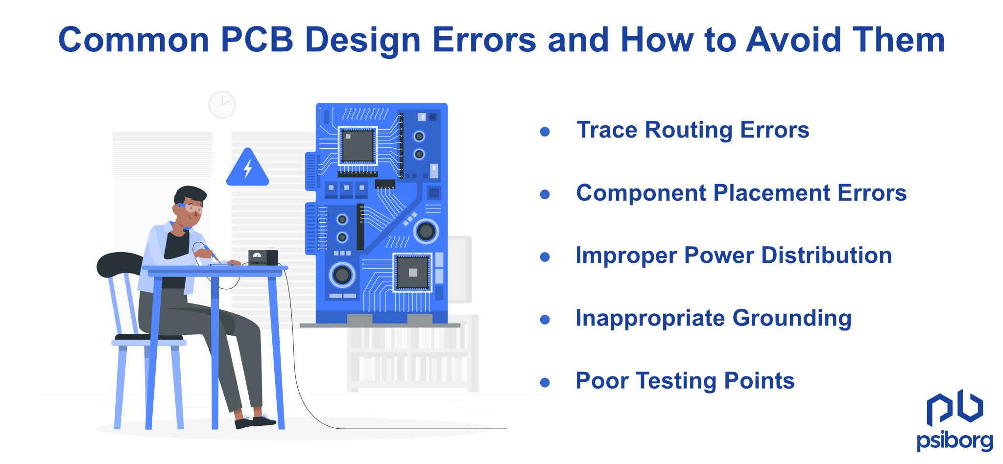
5 Common PCB Design Errors
1. Trace Routing Errors
Routing errors occur when traces are improperly connected or cross each other, leading to short circuits or signal interference.
To avoid this, plan your PCB layout carefully, use a grid system for alignment, and consider signal paths early in the design process. Manually verify routing and use auto-routing tools cautiously.
2. Component Placement Errors
Poor component placement can lead to longer trace lengths, signal degradation, and difficulties in assembling the PCB.
So, carefully arrange components for optimal signal flow, minimize trace length, and avoid placing heat-sensitive components near heat sources like power components or voltage regulators.
3. Improper Power Distribution
Poor power distribution can result in voltage drops, noise, and erratic behavior of components.
You should design a robust power distribution network with sufficient copper thickness and strategically place decoupling capacitors to stabilize voltage levels.
4. Inappropriate Grounding
Grounding issues can introduce noise and interfere with signal integrity.
So make sure to implement a solid ground plane, connect all ground points together, and use separate analog and digital ground regions to reduce noise interference.
5. Poor Testing Points
Lack of test points and programming headers can hinder debugging and testing during production.
To avoid this PCB design error, you can include test points and programming headers in your design to facilitate testing and programming.
How to Avoid Common PCB Design Errors?
If you wish to design reliable, fully-efficient, and functional PCBs, then you should avoid the above-mentioned common PCB design errors. As these silly mistakes can affect your PCB design quality, performance, and cost.
Now that you are aware of some common PCB design errors, let’s discuss some best practices on how to avoid common PCB design errors and upscale our engineering skills.
1. First and Foremost, Plan Your Layout
Before diving into the design, thoroughly understand the project requirements, component specifications, and constraints. It means defining your board’s size, shape, layer, power requirement, and signal integrity.
Planning all this initially will help you optimize space and prevent you from creating routing issues.
2. Use Quality PCB Design Software
Invest in professional PCB design software that offers design rule checking (DRC) and electrical rule checking (ERC) to catch errors early. This way, the chances of getting PCB design errors will be reduced.
3. Use Component Libraries
Always use accurate and up-to-date component libraries to avoid incorrect footprints and symbols. This is considered the easiest way to avoid PCB design errors. As these component libraries and templates will save plenty of your time and effort, plus they will also offer consistency and accuracy in your designs.
4. Follow Schematic Design
Create a well-organized and clear schematic with proper labeling, net names, and hierarchical design if needed. The majority of PCB design software tools come with built-in design rules that check your layout for any errors and violations. Make sure to follow these rules in order to customize them as per your specific needs and standards.
5. Review and Maintain Documentation
Maintain comprehensive documentation, including schematics, BOM, design notes, and assembly instructions, for clarity and future reference.
By proper design review and documentation, you can improve your design skills, and can effectively communicate your design intent. Proper documentation will also facilitate your future modifications and revisions.
Make sure you follow all the above-mentioned points. Considering these points will help you design a successful PCB in the very first attempt.
However, if you still fail to do so, let the experts handle it for you. You obviously don’t want to end up with a costly prototype that is ineffective and takes longer to market.
As an IoT Solution Provider and PCB designer, PsiBorg Technologies is a company with expertise in IoT. If you need help with PCB design or IoT Consulting Services, we can help.


